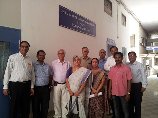
About CNNP
The MEMS and Microelectronics programme has been sustained by IITM along with sponsored research for the last forty years and was also part of the Interdisciplinary Research programme (IDRP) introduced by IITM in 2002. The Photonics programme was especially started in 2001 with an initial grant from IITM alumnus Gururaj Deshpande, Chairman of Sycamore Networks, USA and has grown successfully with several significant achievements to their credit. In 2011 a generous funding was received from MeitY to set up a Centre for Nanoelectromechanical Systems (NEMS) and Nanophotonics (CNNP) that addressed two important branches of Nanotechnology: Nanoelectromechanical systems (NEMS) and Nanophotonics, which are closely related to developments in Nanoelectronics. We have successfully set up nanofabrication and characterisation facilities in about 5000 sq. ft Class 1000 Clean room space, including a Class 100 space for lithography, at IITM. Through the research and development in the first phase, we realised a major part of our work leading to various components like RF switches, sensors, membranes, lamellar gratings, silicon photonics devices, resonators, and others. In the second phase of funding received jointly from MeitY, DST and IITM, under NNetrA programme, we augmented the facilities and focused on systems based on these sensors and components. The facilities added and expertise generated during the first phase of the CNNP have enhanced our capability to work in the areas of NEMS and Nanophotonics and brought in participation from many allied departments. Collaboration with Material Engineering, Biochemists, Mechanical Engineers, Instrumentation and Circuits faculty has enabled our work towards systems building.
Users Feedback
Dr. Gourab Datta, Assistant Professor
CNNP of IITM is one of India's state-of-art facilities for the fabrication and characterization of electronic and optoelectronic devices. During my Ph.D. work, I have extensively used the CNNP facilities. This center is ideal for doing interdisciplinary research.

Dr. Sujatha L, Professor
We, at Rajalakshmi Engineering College, regularly use the services offered by CNNP for our sponsored research projects. We highly depend on the sophisticated equipment available at CNNP for our microfabrication and characterization. The lab technicians and research scholars of CNNP are very supportive during the services. The charges are nominal and it is only 50 percent for academic institutions and hence we are able to pay from projects. We also interact with Professors for technical clarifications. We thank CNNP for their dedication in their services and wish CNNP to continue and expand their services in future.
Dr. Sujith Chandran, Research Scientist ASIC Lab
University of Southern California, USA
CNNP owns a state-of-the-art fabrication facility for microelectronics and nanophotonics research. The most advanced systems such as electron-beam lithography, inductively coupled dry etching system, and high-resolution optical spectrum analyzer enables every possible research in the area of nanophotonics. Hands-on experience from the CNNP facility has been the most valuable skill set for my silicon photonics research.

Dr. Pankaj Arora, Assistant Professor
Department of Electrical Electronics Engineering, BITS, Pilani
During the initial phase of my research career, where the nature of my work was quite uncertain, the CNNP project enabled me an exposure to the state of the art fabrication and characterization facilities. The CNNP project offered clean room fabrication facilities and protocols, quite similar to the leading fabrication facilities outside India. This also facilitated the completion of my thesis and the experience and exposure made quite a positive impact with a lot of appreciation from Prof.Uriel and the group, where I pursued my post-doctoral work. The CNNP project in my opinion is a very promising fab facility to take up advanced research work related to nano and photonics studies in India.
Dr. Sumi Radha Krishnan, Postdoc Researcher
Photonics Research Lab, University of Maryland, USA
I feel privileged to use the state of the art CNNP facilities as part of my PhD program. I realized its relevance when I joined for my post-doc in USA where there are only few equipment that I haven't worked with in IIT Madras.

Dr. Raghu Dharmavarapu, Senior Lead Engineer
SAIT India, Bangalore
I worked at the CNNP during my MS and Ph.D. and I am really happy and proud that I got this opportunity. During my Ph.D., we were the first group to design and fabricate optical Meta surfaces in India, which would not have been possible without such advanced lithography facilities that are available to us at CNNP. As someone who has worked at other world-class fabrication facilities such as MCN(Melbourne), I can proudly say that our CNNP is at par with other advanced academic fabrication facilities and improving with time.

Riddhi Nandi (PhD Thesis Submitted)
Principal Engineering Design Enablement, Global Foundries, Bangalore
The facilities are providing ample scope to students to learn and do hands-on silicon fabrication technologies by staying in their own country. This is clearly advantageous in the long run as the students become at par with other international students and sometimes even outgrow them.