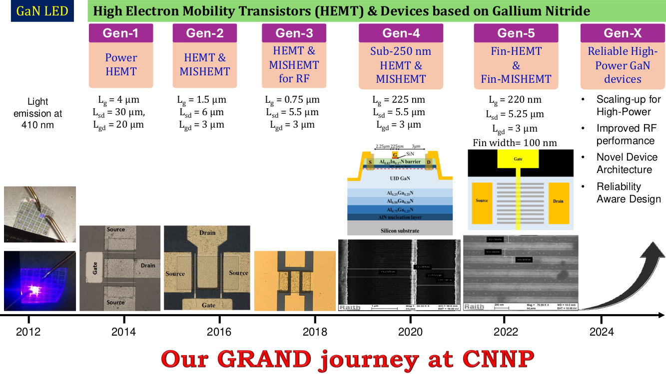
Gallium Nitride and Wide Band-Gap Device Research
Post silicon, Gallium Nitride (GaN) has emerged as the WONDER material that has the potential to disruptively change the future of semiconductor devices. Bolstered by its unique material and device properties, it is finding extensive applications both in power and RF domains; e.g. 5G, Power switches,etc. This technology is expanding to capture the market of electric vehicles, besides being pushed towards application in extreme environments (automobiles, low earth orbit satellites, high temperature and radiation hard application) and even for quantum computing.
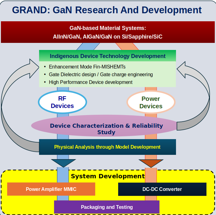
At CNNP, GRAND group works towards development of indigenous GaN technologies and systems through detailed physical analysis, to meet the nations need for a sustainable and prosperous future.
GaN GRAND Research
Key Research Areas
- Indigenous development of GaN device technologies for power and RF applications
- Study of gate leakage mechanisms in HEMTs and MIS HEMTs
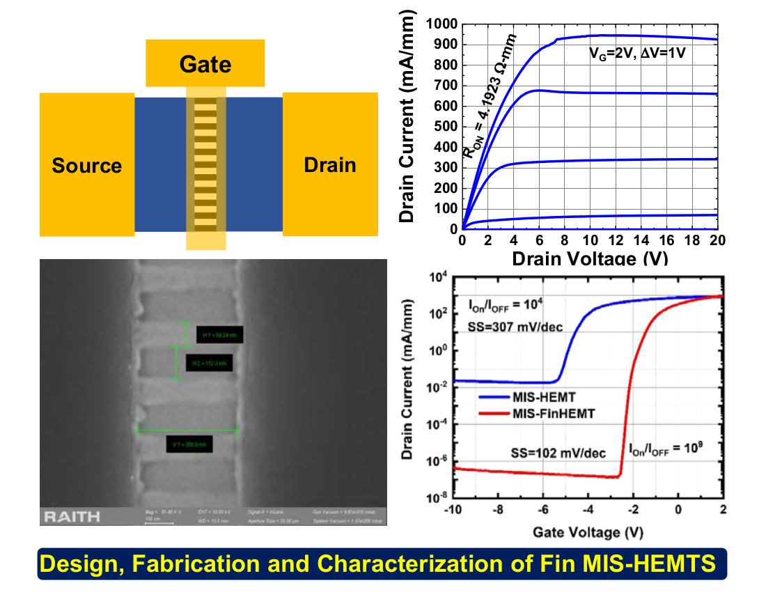
- Enhancement-mode device using charge engineering in Gate dielectric
- Indigenous technology development of Fin-MISHEMT with positive Vth of 0.63V
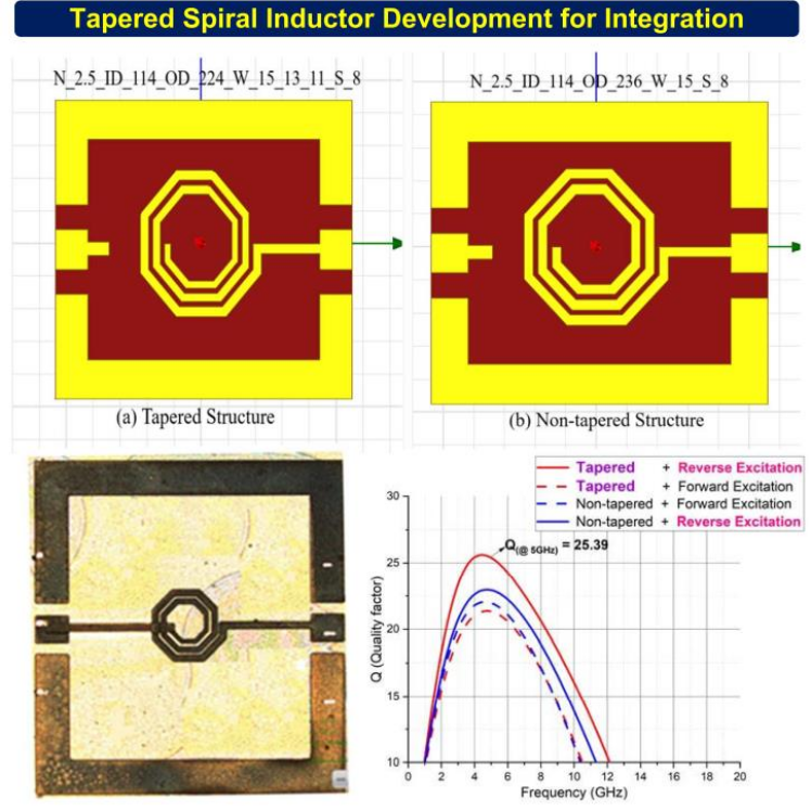
- Development of GaN-based Passives for enabling Monolithic Integration
- Design of Spiral Inductors and capacitors to meet the required specifications for GaN based systems, such as power amplifier
- Fabrication and Characterization of Tapered Spiral Inductors
- Creation of library for GaN-based inductors ranging from 0.5 – 2 nH
- Device characterizations and Reliability Analysis of developed GaN-based devices for better reliability-aware designs
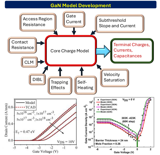
- Compact model for HEMTs developed and validated with available experimental data, both in-house and industrial
- Salient features of developed Model
- Unified and continuous expression for 2-DEG charge versus Gate Voltage
- Accurately predicts DC and AC characteristics
- Includes secondary effects in the core model
- Few number of parameters
- Simple parameter extraction strategy
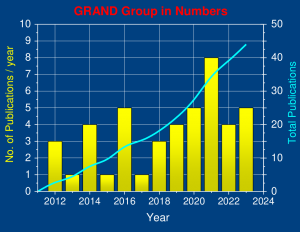
- Publications
- >25 papers in top Journals
- Regular contributions in top conferences
- Total citations >500
- Invited/Keynote Talks
- Invited and keynote talks in several international conferences/workshops
- Manpower Development
- >20 Doctoral and Masters Research scholar trained
- >30 technical staffs trained
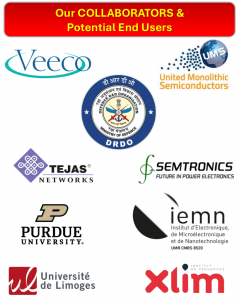
- Industrial Collaborations & End Users
- Veeco Instruments Inc., USA
- United Monolithic Semiconductors (UMS), France
- Solid State Physics Laboratory (SSPL), Defence Research & Development Organisation (DRDO), New Delhi, India
- Tejas Networks, India
- Semtronics, UK
- Academic Collaborations
- Purdue University, USA
- University of Limoges and XLIM, CNRS, France
- IEMN, CNRS, France
Our 10 year VISION
- Create a GaN and Wide Band gap material Research Facility comparable to the best in the world doing cutting edge research
- A Centre which will work closely with industry to provide solutions
- A self-sustainable Centre with a large number of faculty and students
- Provide trained manpower for industry
- Scale up our current technologies to meet industry and market demands
- Work towards developing novel and reliable GaN and Wide Band gap material-based technologies